An increasing number of power electronics products are taking advantage of a growing trend in the printed circuit board industry.
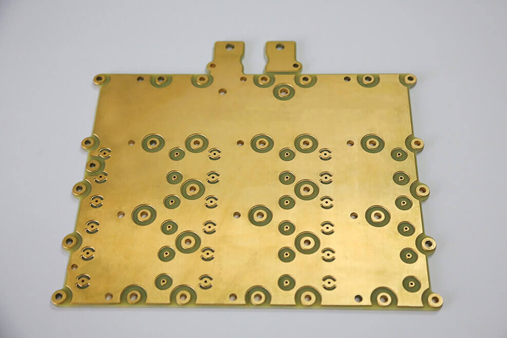
PCBs with 3oz or more of finished copper in the inner and/or outer layers are defined as Heavy Copper. Our manufacturing facilities allow Heavy Copper boards to be produced up to 32 layers.
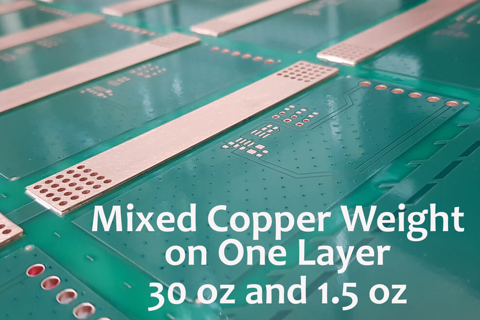
We also have the capability for Extreme Heavy Copper - up to 30oz per layer for 2 layer applications.
Heavy Copper and Extreme Heavy Copper PCB's offer benefits such as:
TCL Elektronika can help you with design procedures for Heavy Copper. We can offer track and gap spacing guidance, current carrying details and best practice guidelines for heavy copper circuits.
Please contact us for further assistance.
TCL (Europe) Elektronika Kft.
120-122 Rona Street,
1149 Budapest,
Hungary
+36-14-683970
sales@tclelektronika.com


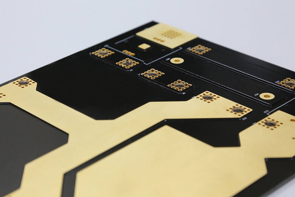
TCL Elektronika can manufacture PCBs ranging from single-sided to complex boards in excess of 40x layers. Our in-house CAM engineering resource allows us to rapidly check, panelise and commercially optimise a fast turnaround prototype as well as small volumes.