Choosing a ceramic substrate for a PCB design is becoming more popular. High maximum operating temperatures of 800°C+ allows for the much higher operating temperatures Silicon Carbide and Gallium Nitride Semiconductors can now operate at. The new DPC (Direct Plated Copper) method of production also allows for through hole plating, miniaturisation and microelectronics not possible with other methods. Ceramics are UV resistant and their inert nature also makes these substrates ideal when a hermetic package is required when no outgassing or moisture can be tolerated.
Low signal loss makes ceramics ideal for high frequency applications but the superior thermal conductivity of up to 180W/mK is often why designers are turning to ceramics.
Advantages Over Other Technologies
Other PCB substrates such as FR4 and Metal Clad PCBs simply do not have the same heat dissipation properties of ceramics. With no isolation layer necessary components are mounted directly onto the boards making the flow of heat through the circuit much more efficient. Depending on substrate choice ceramics offer Thermal Conductivity values ranging from 24-180W/mK. This is matched by excellent CTE (Coefficient of Thermal Expansion) values.
Advantages include:
Available Ceramic Substrates
Ceramic Material Specifications
| Property | Unit | Al2O3 (96%) | Al2O3 (99.6%) | AlN | SiN |
|---|---|---|---|---|---|
| Thermal Conductivity | W/mK | 24 | 29 | 180 | 85 |
| Maximum Operating Temperature (MOT) | °C | >800 | >800 | >800 | >800 |
| Coefficient of Thermal Expansion (CTE) | x 10¯6/K | 6.7 | 6.8 | 4.6 | 2.6 |
| Dielectric Constant | - | 9.8 | 9.9 | 9 | 9 |
| Signal Loss | x 10¯3 | 0.2 | 0.2 | 0.2 | 0.2 |
| Light Reflectivity | % | 70/85 | 75 | 35 | - |
| Dielectric Strength | KV/mm | ≥15 | ≥15 | ≥15 | ≥15 |
| Rupture Strength | Mpa | 400 | 550 | 450 | 800 |
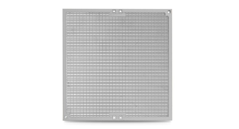
Alumina Oxide (Al2O3) PCB (96% & 99.6%)
The most popular ceramic with a Thermal Conductivity in the region of 24W/mK, a higher figure than the best performing Metal Clad PCB materials.
Available in two different, the 96% being the most cost effective and popular. The 99.6% variant has a higher Thermal Conductivity, in the region of 29W/mK.
Advantages
Technical Specifications
Download our complete design rules below. If you have different requirements, or have any questions please contact us.
Aluminium Nitride (AlN)
If the driver in a design is high thermal conductivity then Aluminium Nitride (AlN) will be the right choice. AlN has a superior thermal conductivity of upto 180W/mK.
With its high temperature and a very low CTE makes AlN suitable for a variety of applications including Semiconductors, High power LEDs, testing and sensors.
Advantages
Technical Specifications
Download our complete design rules below. If you have different requirements, or have any questions please contact us.
| Property | Unit | SiN |
|---|---|---|
| Thermal Conductivity | W/mK | 85 |
| Maximum Operating Temperature (MOT) | °C | 1000 |
| Coefficient of Thermal Expansion (CTE) | x 10¯6/K | 2.6 |
| Dielectric Constant | - | 9 |
| Signal Loss | x 10¯3 | 0.2 |
| Light Reflectivity | % | - |
| Breakdown Voltage | KV/mm | 15 |
| Rupture Strength | Mpa | 800 |
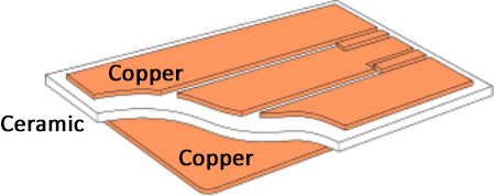
Active Metal Brazing (AMB) - Ceramic PCBs
A new production method of manufacturing ceramics without metallisation is known as Active Metal Brazing (AMB)
In a vacuum, using high temperatures AMB 'brazes' the copper direct to the ceramic substrate.
AMB produces an extremely reliable substrate with unique heat dissipation properties.
The brazing method enables copper weights of up to 800µm to be produced on very thin ceramic substrates making it ideal for Power Electronics applications.
AMB Single Sided
The table below shows the copper weights that are available with the corresponding substrate thicknesses. For mechanical stability it is always recommended the copper thickness is no more than half the ceramic thickness.
AMB Double Sided
With copper both sides a higher stability and mechanical strength is achieved enabling Heavy Copper to be offered on thin ceramic substrates. The following is a guide on double sided material availability although during the etching process original copper weights can be reduced.
| Active Metal Brazing Double Sided Panels | ||||||
|---|---|---|---|---|---|---|
| 200µm | 250µm | 300µm | 400µm | 500µm | 800µm | |
| 0.25mm | SiN AlN |
SiN AlN |
SiN | SiN | SiN | SiN |
| 0.32mm | SiN | SiN | SiN | SiN | SiN | SiN |
| 0.38mm | AlN | AlN | AlN | |||
| 0.63mm | AlN | AlN | AlN | AlN | AlN | |
| 1.00mm | AlN | AlN | AlN | AlN | AlN | AlN |
Ceramic - Thick Film
Ceramics - DBC (Direct Bonded Copper)
Disadvantages:
Applications:
Main applications are high power modules, like IGBT, CPV, or any other wide bandgap device modules.
Ceramics - DPC (Direct Plated Copper)
Applications:
Ceramics - DPC vs DBC
Both DBC and DPC have the same advantages for high power applications, due to the use of a direct bond between Copper and the Ceramic substrate, therefore, the same key attributes for both of them are:
The differences come when looking at the design considerations and applications. DBC being suited to high current capacity, however limited on circuit design. DPC allowing for finer tracks and through hole connection.
Ceramic - Capabilities
| Property | DPC | DBC |
|---|---|---|
| Compatible Substrates | Al2O3 / AlN / SiN | Al2O3 / AlN / SiN |
| Substrate Thickness (mm) | 0.25/0.38/0.5/0.635.1.0/1.5/2.0 | 0.25/0.38/0.5/0.635.1.0/1.5/2.0 |
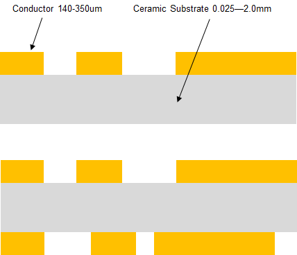
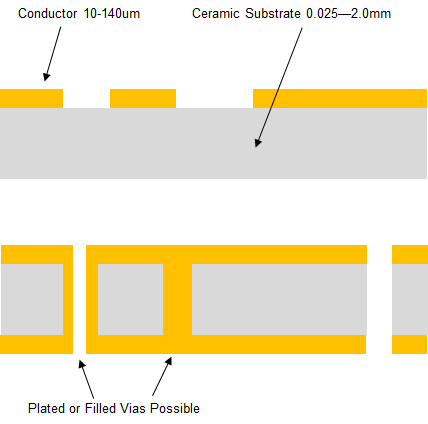
| Copper Weight (oz) | 10 - 140 | 140 - 350 |
| Panel Sizes (mm x mm) | Standard: 115 x 115mm Special: Up to 170 x 250mm |
Standard: 115 x 115mm Special: Up to 170 x 250mm |
| Finish Options | ENIG/ENEPIG/EPIG/Immersion Silver/Immersion Tin/OSP | ENIG/ENEPIG/EPIG/Immersion Silver/Immersion Tin/OSP |
| Min Track Width (mm) | 0.1 | Dependant on Cu Weight |
| Minimum Hole Dia (mm) | 0.08 | 0.08 |
| Plated Via Aspect Ratio | 5:1 | N/A |
Some of the surface finishes common with standard substrates such as FR4 are not suitable for ceramics. The finishes we offer are shown below. We would be happy to discuss with you further what might be a suitable finish for your boards.
Usual thickness : 0.20-0.65µm
Shelf Life : 6 months
Unprotected copper will quickly oxidise which can cause soldering issues. OSP is a popular, low cost, environmentally friendly finish to prevent that oxidisation and provide an improved surface for solderability.
The main benefits of using ceramics is heat management. Ceramics are also specified for high frequency applications due to the low signal loss. Many high-power packages require substrates that can sustain high operating temperatures. Ceramic substrates from TCL feature high Thermal Conductivity values of up to 180W/mK and a maximum working temperature of over 800°C. They also offer advantages for hermetic applications because of their 0% water absorption and extremely low CTE (Coefficient of Thermal Expansion).
Depending on the ceramic substrate you choose thermal conductivity is available between 24-180W/mK
Al2O3 (Alumina Oxide) - 96% is the most common substrate and a very cost-effective option and has a Thermal Conductivity of around 24W/mK.
When Thermal Conductivity is the main consideration, AlN (Aluminium Nitride) is frequently chosen. It is the ideal choice for systems with high thermal demands because of its Thermal Conductivity of 180W/mK.
SiN (Silicon Nitride) is more shock-resistant than other substrates due to its increased fracture toughness and bending strength. As a result, it is an excellent option for automotive applications where structural durability is crucial.
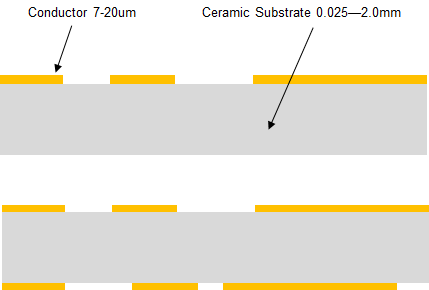
DPC. The most recent advancement in the field of Ceramic Substrate PCBs is Direct Plated Copper (DPC). This production technique can produce copper thicknesses ranging from 10µm ( 1/3oz) to 140µm (4oz). After a procedure known as vacuum sputtering bonds a thin layer of copper on the substrate, the copper is plated up to the desired thickness and the PCBs are then etched. With this method we can produce fine tracks, excellent tolerances and through hole plated holes.
DBC. The traditional method of ceramic circuit production is Direct Bonded Copper (DBC). It is often used when a high copper thickness is required, often between 140µm (4 oz) and 350µm (10oz). A high-temperature oxidation method is used to bond the copper to the ceramic substrate on either one or both sides. The copper circuit is achieved by conventional PCB fabrication techniques to etch away unwanted copper. However, depending on the required copper weight, this production method may limit track widths and gaps due to etch tolerances. Through hole plating is not available with DBC.
Standard production panel sizes are 115 x 115mm but special panels can be used up to 170 x 250mm. After allowing for tooling the usable area from these panels is 105 x 105mm and 160 x 240mm.
HASL is not suitable, so the finishes available are: ENIG/ENEPIG/EPIG/Immersion Silver/Immersion Tin and OSP.
High Thermal Conductivity of up to 180W/mK, operating temperatures of the substrates of over 800°C, low CTE (Coefficient of Thermal Expansion) low signal loss for high frequency applications and 0% water absorption for Hermetic packages.
AMB uses a unique production method where the copper is directly attached (brazed) to the ceramic substrate in a high temperature vacuum. AMB enables copper weights of up to 800µm on thin ceramic substrates. It is ideal for Power Electronics applications.
Using traditional DBC substrates copper to 350µm is available. With DPC we have manufactured panels to 1100µm.
For standard solder resists 130°C is maximum long-term exposure. For assembly, as a minimum, all Solder Resists used pass IPC thermal stress test; 3 times, 288°, 10 seconds.
We can offer a Glass Glaze Solder Mask that can be used at temperatures of up to 500°C. However, this resist is only suitable for silver paste on Alumina (Al2O3). It is not suitable for DBC or DPC construction.
We can supply a panel of ceramic circuits, but the vast majority of our customers ordered singles. The reason for this is ceramics are more brittle than other substrates such as FR4. If required, we can supply laser cut v-score panels for careful manual break-out of the circuits after assembly. If you require non scored panels, then a laser or depaneling machine with a diamond blade should be used.
Ceramic PCBs can be used at a very low temperature. We have manufactured boards without a solder resist or ident for use in a cryogenic chamber at -223°C.
It can. The DPC method of production can be utilised to produce different thicknesses of copper in selected areas. This can be useful if you need thin copper for a control section and thick copper for a power section on the same layer.
A laser is used for drilling and routing ceramic circuits so this can be used for scribing. This is useful if outgassing is a consideration and conventional idents cannot be used.
No, the production method is irrelevant. This is because the roughness of the copper surface is determined by the polishing process after plating. For some products with strict requirements on surface roughness (such as LED, Ra< 0.3µm and Rz< 2µm), our factory will use polishing equipment to treat the copper surface after plating to reach the requirements of low roughness. Therefore, the same roughness requirements can be achieved for both DPC and DBC processes.
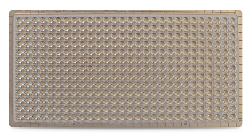 Populated with LEDs
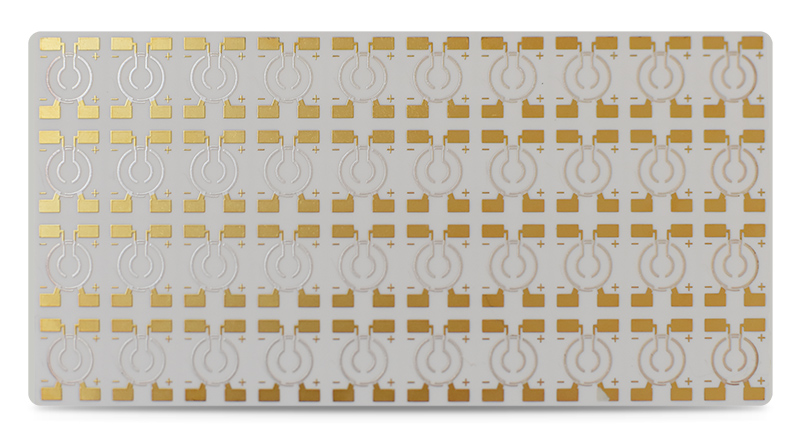 Silver Paste Conductor with ENIG Surface Treatment
 Immersion Tin Panel
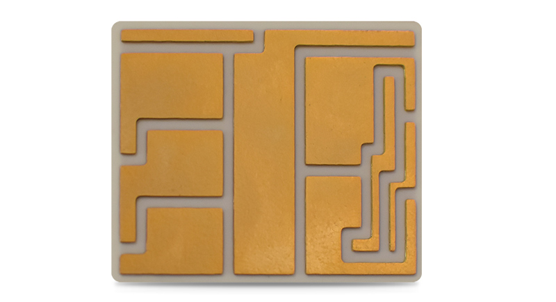
 Alumina Oxide Al203
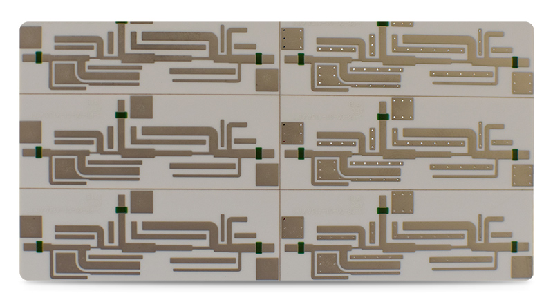
 Direct Bonded Copper
 Alumina Oxide Al203
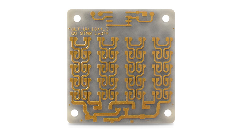 AIN Used For LED Products
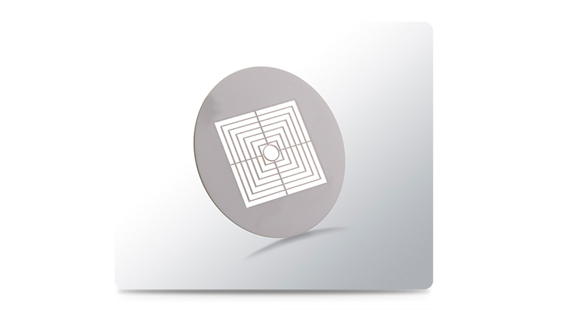
 Saphire Alumina 0.4mm 2 Layer Silver Conductor
 Alumina 0.5mm Silver Fin
TCL (Europe) Elektronika Kft.
120-122 Rona Street,
1149 Budapest,
Hungary
+36-14-683970
sales@tclelektronika.com


TCL Elektronika can manufacture PCBs ranging from single-sided to complex boards in excess of 40x layers. Our in-house CAM engineering resource allows us to rapidly check, panelise and commercially optimise a fast turnaround prototype as well as small volumes.