The advancement of science and technology makes our life easier, but often leads to several problems, especially for printed circuit boards. PCB is closely related to our daily life. Improper handling of printed circuit boards will cause environmental pollution, waste of resources and other problems. Therefore, how to effectively recycle and recycle scrap printed circuit boards has become one of the key issues of the times.
Which industries have printed circuit boards for electronics?
Almost all electronic equipment in various industries is equipped with printed circuit boards, such as computers, televisions, automotive navigation devices, medical imaging systems, etc.
PCB is very common in the following different electronic equipment:
Printed circuit board application industry and classification of its equipment:
A printed circuit board (PCB) allows the creation of large and complex electronic circuits in a small space. In addition to meeting PCB designers' design needs and concepts to achieve highly free electronic component layout and PCB design through manual design (CAD drawing) and automatic design (automatic router), it can also continuously meet various kinds of electronic products as the core component of almost all electronic products Different needs of different consumers.
What is the toxicity of the printed circuit?
PCB design and manufacturing is mainly in the copper clad laminate to remove excess copper and form a circuit, the multilayer PCB also needs to connect each layer. As the printed circuit board is finer and finer, the processing accuracy increases, resulting in more and more complex PCB manufacturing. Its manufacturing process has dozens of processes, each process has chemicals in the wastewater. Pollutants in wastewater from PCB design and manufacturing are as follows:
Since the circuit is left behind by removing excess copper from the copper clad laminate, copper is the main pollutant in PCB design wastewater and copper foil is the main source. Furthermore, given the need to conduct the circuit of each layer of double-sided panel and multilayer panel, the circuit of each layer is conducted by drilling holes and copper plating on the substrate, while the first layer of copper plating on the substrate (usually resin) and non-electrolytic copper plating is used in the intermediate process.
Non-electrolytic copper plating uses complex copper to control stable copper deposition rate and copper deposition thickness. EDTA Cu (sodium copper) is commonly used, but there are also unknown components. PCB cleaning water after electrolysis copper plating also contains complex copper. Also, there are nickel plating, gold plating, tin plating, and lead plating in PCB manufacturing, so these heavy metals are also contained.
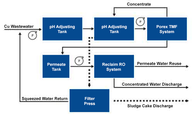
In the process of creating circuit graphics, etching copper sheets, soldering circuits, and so on, the ink is used to cover the copper sheet that needs to be protected, then it is returned. These processes produce a high concentration of organic matter, some COD up to 10 ~ 20g / L. These highly concentrated wastewater accounts for about 5% of the total water and is also the main source of COD in the production wastewater. of PCB. * PCB Production Wastewater Treatment (Source: Porex Filtration)
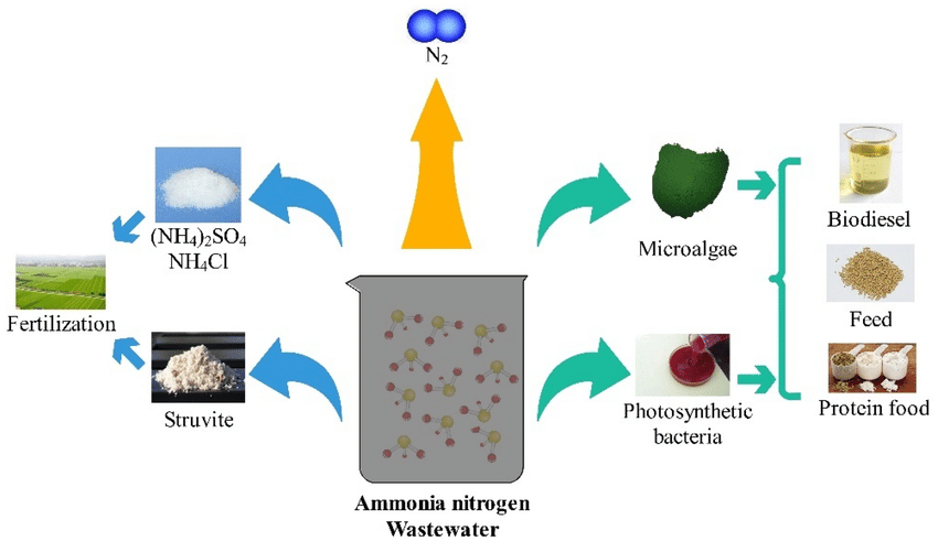
Depending on the different manufacturing processes, some processes contain ammonia, ammonium chloride, etc. In the etching solution, which is the main source of ammoniacal nitrogen. * Recovery of ammonia-nitrogen from wastewater and its use (Source: Researchgate)
Other pollutants
In addition to the main pollutants mentioned above, there are acid, alkali, nickel, lead, tin, manganese, cyanide ion and fluorine. In the manufacture of PCBs, sulfuric acid, hydrochloric acid, nitric acid, and sodium hydroxide are used. There are dozens of commercial solutions, such as etching solution, non-electrolytic plating solution, electroplating solution, activation solution and prepreg. The components are complex. In addition to most of the known components, there are some unknown components, which makes wastewater treatment more complex and difficult.
Useful content in the printed circuit
General military electronic equipment or civilian electronic equipment is equipped with printed circuit boards, which contain a variety of recyclable precious metals and important electronic components, some of which can be decomposed, recycled and reused, such as silver, gold, palladium and copper. In the recovery process, the recovery rate of these precious metals can reach 99%.
How to recycle printed circuit boards?
There are three main ways
They have pros and cons based on how the metal will be recycled Let's look.
Metal separation technology
Wastewater from PCB manufacturing contains a high level of Cu2 + and a small amount of other metal ions (mainly Zn2 +). Separating Cu ions from other metals can improve the purity of the recycled copper. A D4EHPA modified Amberlite XAD-2 resin prepared with the solvent-non-solvent method can remove the Zn ions, leaving the Cu ions in the solution. The ion exchange isotherm showed that the D4EHPA modified Amberlite XAD-2 resin has a higher Zn ion selectivity than the Cu ion. The results of the selective extraction demonstrated that Amberlite XAD-2 resin modified with D4EHPA can separate the Zn / Cu mixed ion solution. After ten batches of contacts, the relative Cu ion concentration increases from 97% to more than 99.6%, while the relative Zn ion concentration decreases from 3.0% to less than 0.4%.
PCB recycling: what can you recycle?
Recycling of waste printed circuit boards is expensive. Only the metal part of the circuit board has a reuse value, so the non-metal part needs to be separated from the electronic waste, which is an expensive process.
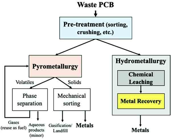
There are many ways to recycle waste printed circuit boards. It includes hydrometallurgical and electrochemical processes. Many of these methods contribute to the recovery of scrap precious metals, electronic components, and connectors.
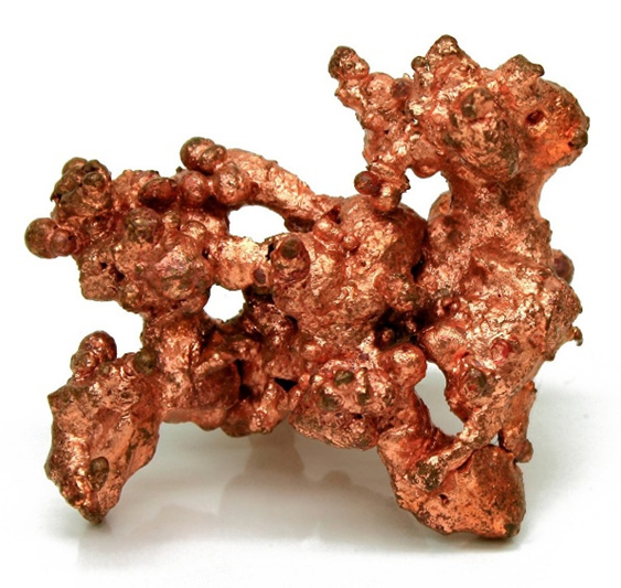
Take copper as an example. As one of the precious metals with a high recovery value, copper can be reused in a variety of applications. The first advantage of copper is its high conductivity. This means that it can easily transmit signals without losing power along the way. It also means that manufacturers don't have to use a lot of copper. Even a small amount of work can be done. In the most common configuration, one ounce of copper can be transformed into 35 microns (about 1.4 inches thick), covering the entire square foot of a PCB substrate. Copper is also readily available and relatively inexpensive.
Recycling of resource-rich waste generated by the printed circuit board industry includes
(1) recovery of metallic copper from the edge of printed circuits
(2) recovery of tin metal from tin / lead slag in the hot air levelling process
(3) recovery of copper oxide from sewage treatment sludge
(4) recovery of copper from the basic etching solution
(5) recovery of copper hydroxide from copper sulphate solution in the plated through hole (PTH) process
(6) copper recovery from the rack stripping process
(7) recovering copper from the tin / lead stripping solution used up in the solder stripping process.
How to make waste printed circuits more recyclable?
As a world-renowned first-class printed circuit board manufacturer and seller, TCL ELEKTRONIKA always pays attention to the manufacturing technology and PCB design capabilities, but at the same time we are also trying to recycle those scrap printed circuit boards, hoping to reduce the impact of this type of electronic waste on the environment and ecology.
Date : 30-11-2021
TCL (Europe) Elektronika Kft.
120-122 Rona Street,
1149 Budapest,
Hungary
+36-14-683970
sales@tclelektronika.com


TCL Elektronika can manufacture PCBs ranging from single-sided to complex boards in excess of 40x layers. Our in-house CAM engineering resource allows us to rapidly check, panelise and commercially optimise a fast turnaround prototype as well as small volumes.