As you well know, there is no standard printed circuit board. Each PCB has a unique function for a particular product. Therefore, the production of a PCB is a complex and multi-stage process. This overview covers the most important steps when manufacturing a multilayer PCB.
When you order your PCBs from TCL Elektronika, you are buying a quality that pays off over time. This is guaranteed by product specifications and quality controls much stricter than those of other suppliers and guarantees a very strict control during the production phase.

The data provided by the customer (Gerber) is used to produce the production data for the specific PCB (artwork for imaging processes and drilling data for drilling programs). Engineers compare requests/specifications with capabilities to ensure compliance and determine the process steps and related controls. Changes are not permitted without our permission.
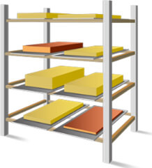
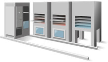
Material of various types is received from approved sources and kept in controlled environments until required. The specific material is released into production for a specific purchase order with the basic materials cut to the required size. All materials used can be traced back to their production batch. We use only internationally known bases.
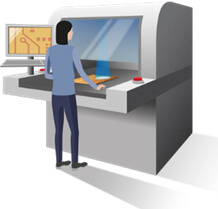
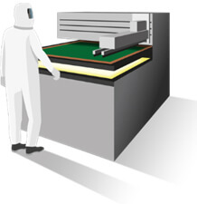
Step 1 consists of transferring the image using a film to the surface of the panel, using photosensitive dry film and UV light, which will cure the exposed dry film. This stage of the process is carried out in a clean room.
Step 2 is to remove the unwanted copper from the panel, using the engraving. Once this copper has been removed, the remaining dry film is then removed leaving behind the copper circuit that corresponds to the design.
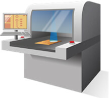
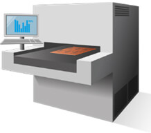
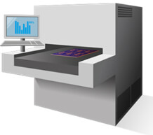
Inspection of the circuits against the digital "images" to verify that the circuits correspond to the design and that they are free of defects, through the scanning of the board and then any anomalies that the scanning process has highlighted will be verified. TCL does not allow the repair of open circuits. All PCBs are tested using TCL approval.
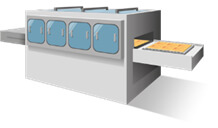
The inner layers have a layer of oxide applied and then "stacked" along with the pre-impregnated that provides insulation between the layers, and the copper foil is added to the top and bottom of the pile. The lamination process uses a combination of specific temperature, pressure for a specific time to allow the resin inside the pre-impregnated to flow and bind the layers together to form a solid multilayer panel.
Now we must drill the holes that will subsequently create the electrical connections inside the multilayer PCB. This is a mechanical drilling process that needs to be optimized so that you can get recording to all connections of the inner layer. Panels can be stacked in this process. Drilling can also be done with a laser drill.
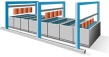
PTH provides a very thin copper deposit that covers the wall of the hole and the entire panel. A complex chemical process that must be strictly controlled to allow reliable copper deposit to plate even on the wall of the non-metallic hole. Although a quantity of copper alone is not enough, we now have electrical continuity between the layers and through the holes.

Panel plating follows the PTH to provide a thicker copper deposit above the deposit, typically 5 to 8 Um. The combination is used to optimize the amount of copper to be plated and engraved to meet the needs of track and distance.
Similar to the process of the inner layer (image transfer by means of photosensitive dry film, exposure to UV light and engraving), but with one main difference: we will remove the dry film where we want to keep the copper/definition circuit, so that we can plate further and copper later in the process. This stage is carried out in a clean room.
Second stage of electroplating, where additional plating is deposited in areas without dry film (circuits). Increase the thickness of the plating to meet the demands. Once the copper has been plated, tin is applied to protect it.
This is normally a three-step process. The first step is to remove the dry film, blue. The second step is to etch away the exposed/unwanted copper while the tin deposit acts as an etch resist protecting the copper we need. The third and final step is to chemically remove the tin deposit from the circuits.
Just like as with the inner layer AOI, the filmed and engraved panel is scanned to make sure that the circuit meets the design and that it is free of defects. Again, according to the demands of TCL, the repair of open circuits is not allowed.
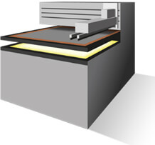
Using soldermask ink or epoxy resin and a stencil preparation, we use a screen printing process to push the ink or resin into the holes. This stage of the process is carried out in a clean room.
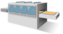
Soldermask ink is applied over the entire surface of the PCB. And we lay out certain areas to UV rays, and those unexposed areas are removed during the chemical development process, typically areas that need to be used as weldable surfaces. The remaining soldermask is then fully cured, making it a durable finish. This stage of the process is carried out in a clean room.
Various finishes are then applied to the exposed copper areas. This is to allow surface protection and good weldability. Various finishes may include Electroless Nickel Immersion Gold, HASL, Immersion Silver etc. Thicknesses and weldability tests are always performed.
This is the process of cutting production panels into specific sizes and shapes according to the customer's design, as defined in the Gerber data. There are 3 main options available when providing the array or selling the panel: scoring, routing, or punching. All dimensions are measured against the drawing provided by the customer to ensure that the panel is dimensionally correct.
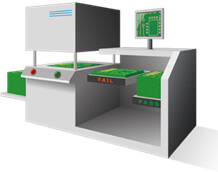
Used to verify the integrity of tracks and through-hole interconnections, verifying that there are no open circuits or short circuits on the finished board. There are two test methods, flying probe for smaller volumes and volume-based device.
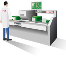
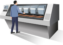
Visual inspection of the PCB against the criteria of acceptance and use of TCL. Using manual visual inspection and AVI, we compare PCBs with Gerbers and it has a faster control speed than human eyes, but still requires verification by one of our operators. All orders are also subjected to a full inspection that includes dimensions, weldability, etc.
The PCBs are packed using compliant materials and shipped using the required mode of transport.
Date : 05-11-2021
TCL (Europe) Elektronika Kft.
120-122 Rona Street,
1149 Budapest,
Hungary
+36-14-683970
sales@tclelektronika.com


TCL Elektronika can manufacture PCBs ranging from single-sided to complex boards in excess of 40x layers. Our in-house CAM engineering resource allows us to rapidly check, panelise and commercially optimise a fast turnaround prototype as well as small volumes.