Back to News List

Ceramics Process Methods

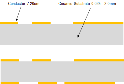
Ceramic - Thick Film

  • Thick Film technology involves the addition of layers of conductor (Copper or Silver) onto a Ceramic substrate via screen printing processes.
  • Suitable for use with Al2O3/AlN and Sapphire substrates.
  • A cost-effective solution with fewer manufacturing processes than other methods.
  • With a conductor thickness between 7-20um it is not well suited to power electronics requiring high current capacity.
  • Due to conductor application it is also unsuitable for designs requiring fine tracks and/or plated/filled vias.
Closeup of Ceramic Thick Film
Ceramic Thick Film Technology - layers of conductor onto a ceramic substrate

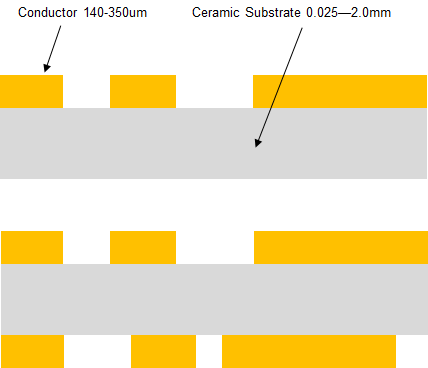
Ceramics - DBC (Direct Bonded Copper)

  • Direct Bonded Copper (DBC) is used when a high copper thickness is required - 140um (4oz)-350um (10oz). Heavy Copper.
  • The copper is bonded to the Ceramic substrate on one or both sides using a high-temperature oxidation process.
  • The copper and substrate are heated in an atmosphere of nitrogen containing about 30 ppm of oxygen; under these conditions, a copper-oxygen eutectic forms which bonds successfully both to copper and the oxides used as substrates.
  • The copper layers can then be etched using standard PCB technology to form an electrical circuit.
  • Laser drilling is then used for any through hole requirements and profile machining.

Disadvantages:

  • Due to the Oxidisation bonding process there can be a slight reduction in Thermal Conductivity created by a void between the Copper and Ceramic layers.
Closeup of Ceramic Direct Bond Copper

Applications:

Main applications are high power modules, like IGBT, CPV, or any other wide bandgap device modules.

  • IGBT
  • High-Frequency Switching Power Supply
  • Automotive
  • Aerospace
  • Solar Cell Component
  • Power Supply for Telecommunication
  • Laser Systems
Closeup of Ceramic Direct Bonded Copper

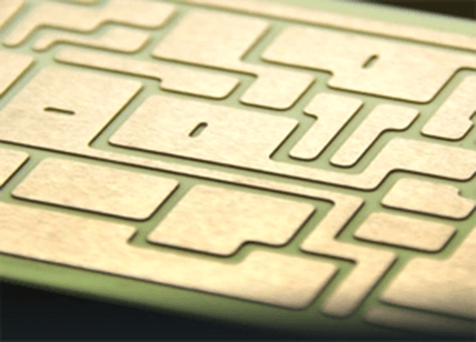
Ceramics - DPC (Direct Plated Copper)

  • Direct Plated Copper (DPC) is the newest development in the field of Ceramic Substrate PCBs.
  • It involves plating the copper conductor layer to the copper substrate under high temperature and pressure conditions.
  • The addition of a thin titanium layer acts as a bonding interface between the copper and Ceramic layers.
  • A very thin layer of Copper is deposited at this stage coating the Ceramic substrate and any pre-drilled holes.
  • Track printing and etching is then performed with the thin Copper allowing for very fine tracks and reduced undercutting.
  • The panels are then plated up to the required end copper thickness.
  • Using this method can result in copper thickness' ranging from 10um (≈ 1/3oz) to 140um (4oz).
  • It also allows for the possibility of plated or filled vias. Something not possible with Thick Film or DBC technology.
Ceramic Direct Plated Copper - layers of conductor onto a ceramic substrate

Applications:

  • HBLED
  • Substrates for solar concentrator cells
  • Power semiconductor packaging including automotive motor control
  • Hybrid and electric automobile power management electronics
  • Packages for RF
  • Microwave devices
Closeup of Ceramic Direct Plated Copper

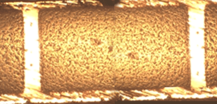
Ceramics - DPC vs DBC

Both DBC and DPC have the same advantages for high power applications, due to the use of a direct bond between Copper and the Ceramic substrate, therefore, the same key attributes for both of them are:

  • Outstanding Thermal Conductivity
  • High operating temperatures
  • Good mechanical strength; mechanically stable shape, good adhesion.
  • Excellent electrical insulation
  • Very good thermal conductivity
  • Superb thermal cycling stability
  • Good heat spreading

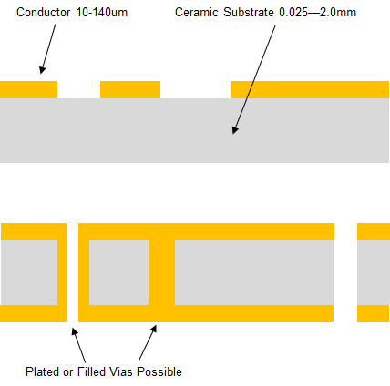
The differences come when looking at the design considerations and applications. DBC being suited to high current capacity, however limited on circuit design. DPC allowing for finer tracks and through hole connection.

Ceramic - Capabilities

Property DPC DBC
Compatible Substrates Al2O3 / AlN / SiN Al2O3 / AlN / SiN
Substrate Thickness (mm) 0.25/0.38/0.5/0.635.1.0/1.5/2.0 0.25/0.38/0.5/0.635.1.0/1.5/2.0
Copper Weight (oz) 10 - 140 140 - 350
Panel Sizes (mm x mm) Standard: 115 x 115mm
Special: Up to 170 x 250mm
Standard: 115 x 115mm
Special: Up to 170 x 250mm
Finish Options ENIG/ENEPIG/EPIG/Immersion Silver/Immersion Tin/OSP ENIG/ENEPIG/EPIG/Immersion Silver/Immersion Tin/OSP
Min Track Width (mm) 0.1 Dependant on Cu Weight
Minimum Hole Dia (mm) 0.08 0.08
Plated Via Aspect Ratio 5:1 N/A

Date : 18-10-2021